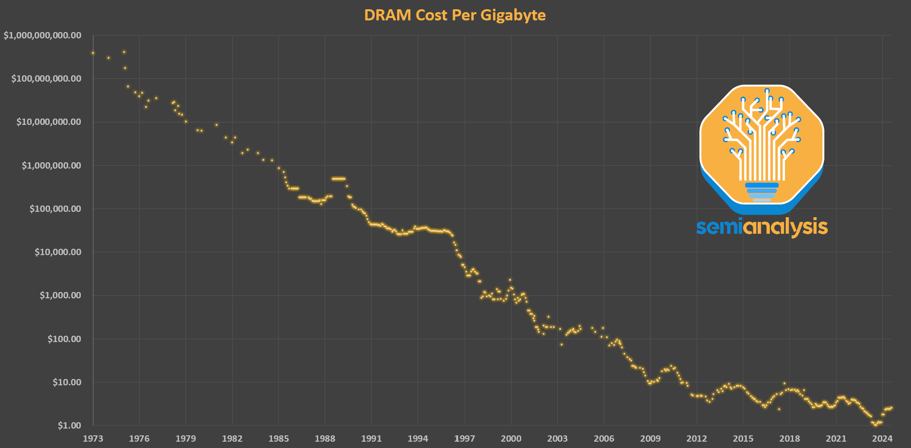
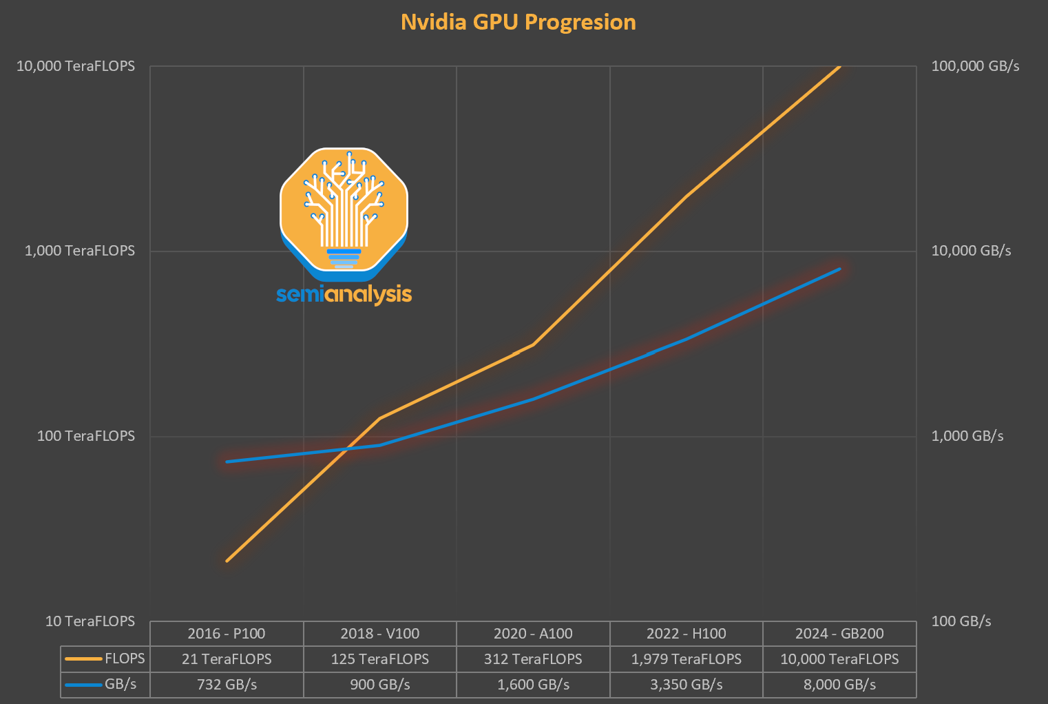
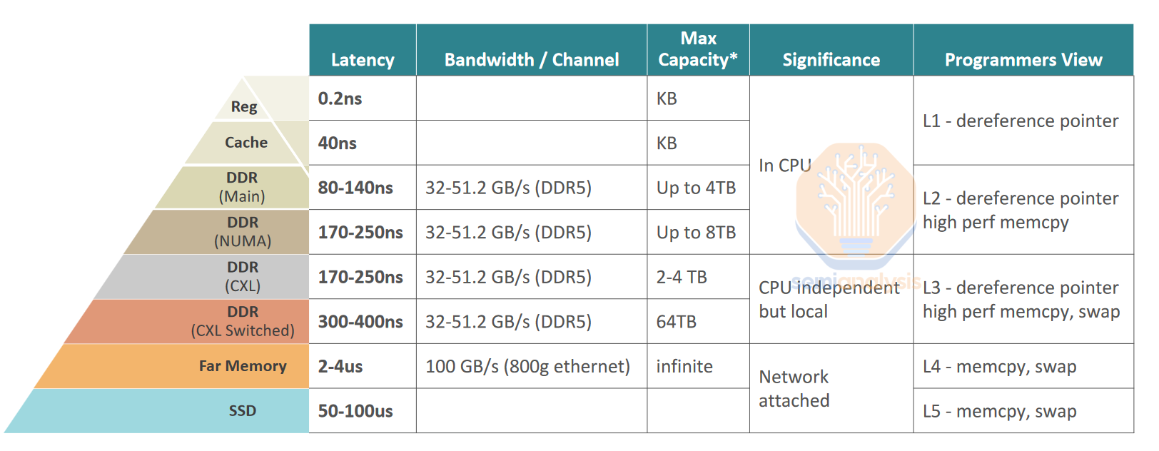
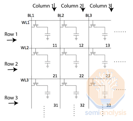
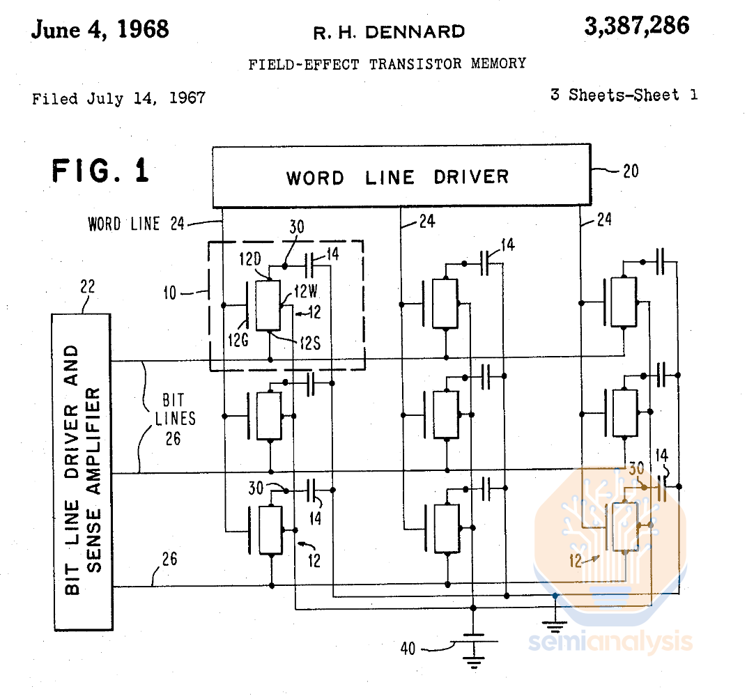
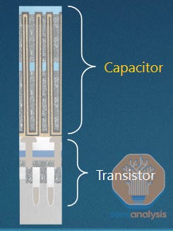
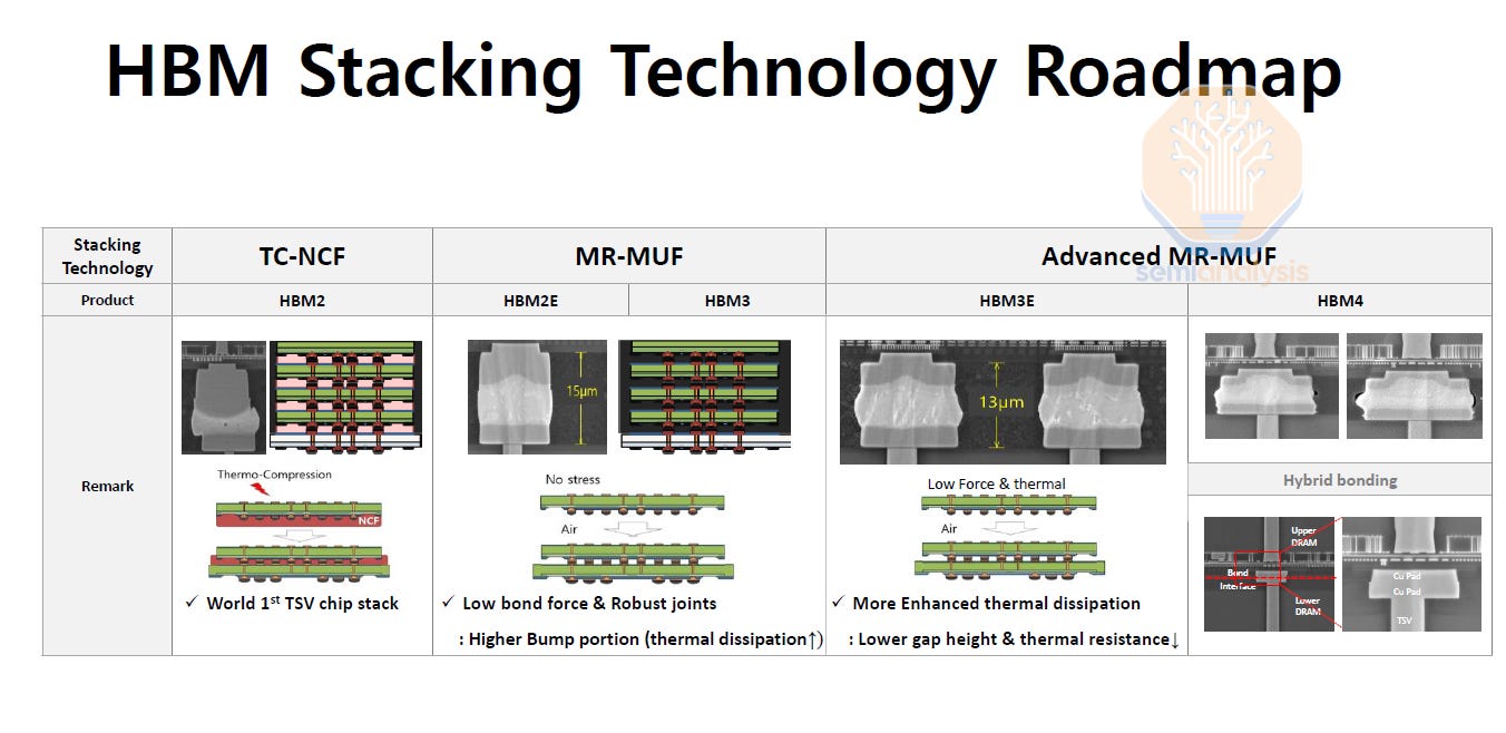
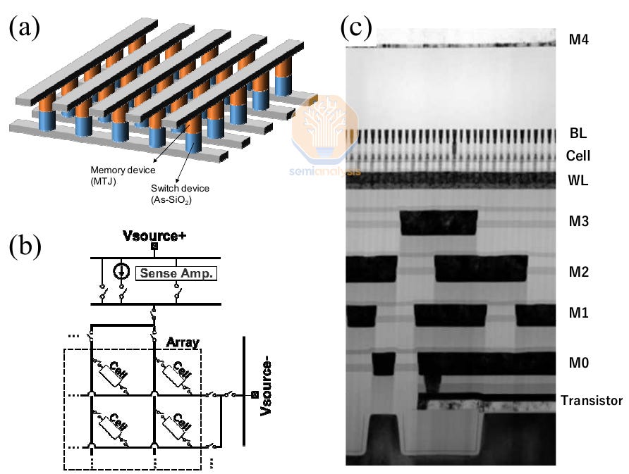
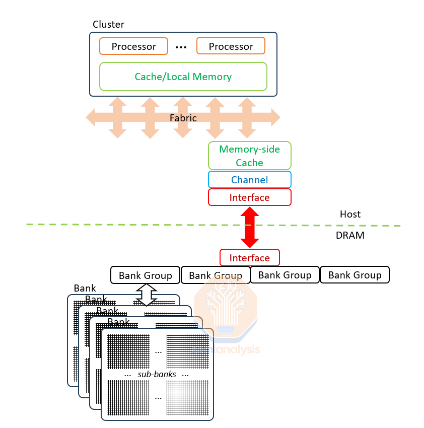
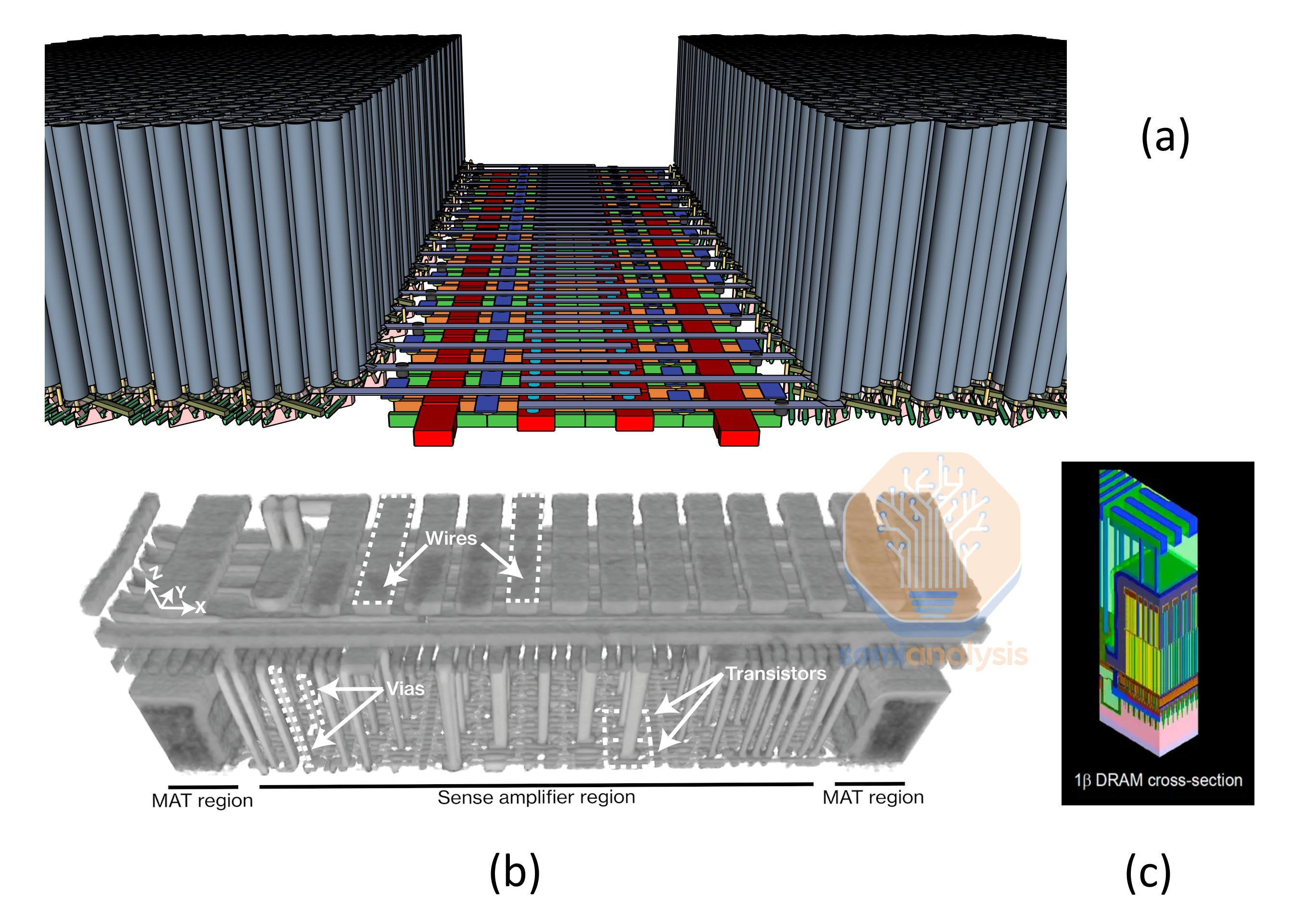
The world increasingly questions the death of Moore’s Law, but the tragedy is that it already died over a decade ago with 0 fanfare or headlines. The focus is generally on logic, but Moore’s Law always also applied to DRAM. 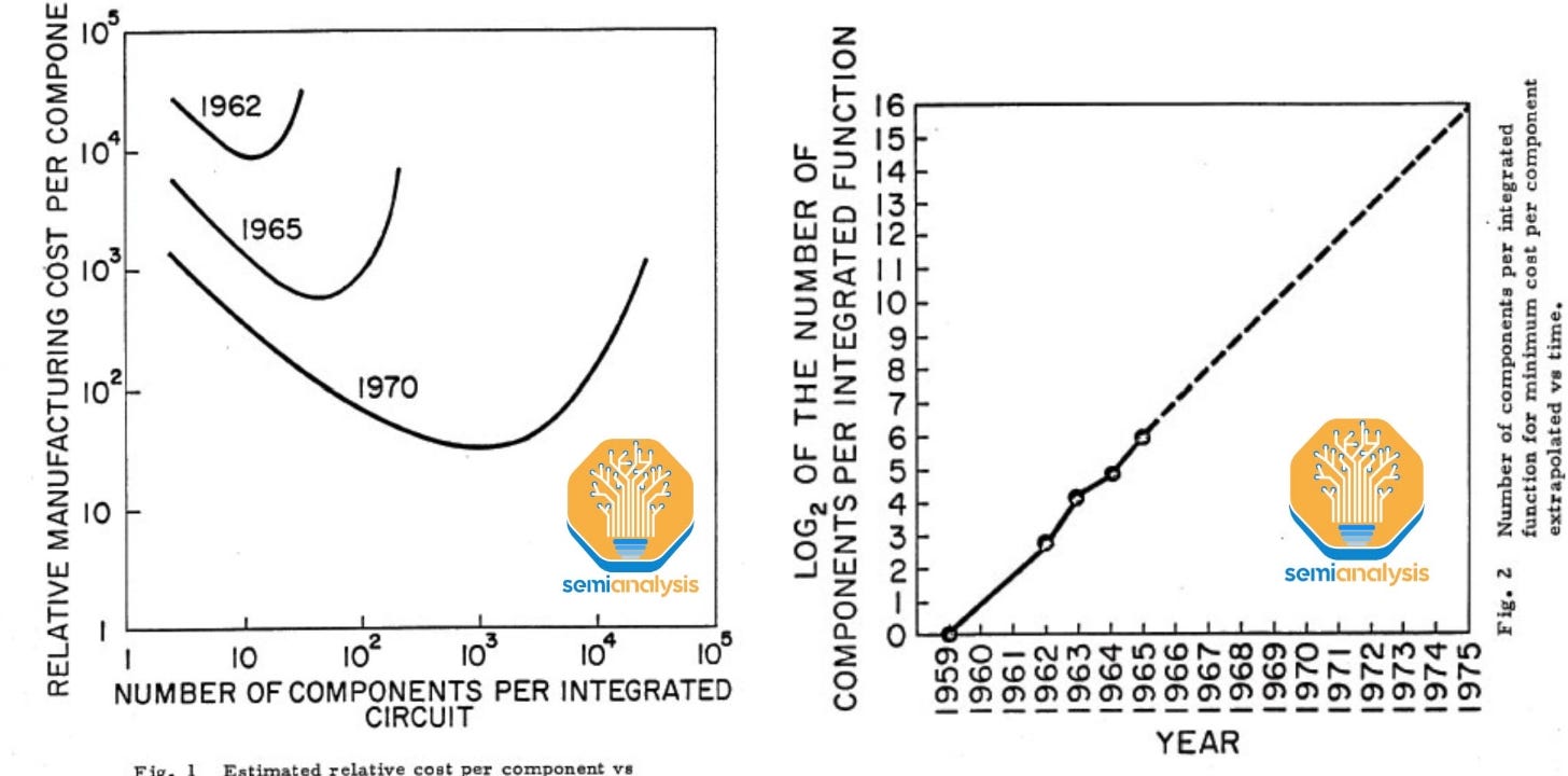 The Original Scaling Laws - Source: 1965 The Future of Integrated Electronics – Gordan Moore DRAM doesn’t scale anymore. In the glory days, memory bit density doubled every 18 months – outpacing even logic. That translates to just over 100x density increase every decade. But in this last decade, scaling has slowed so much that density has increased just 2x. Now with the explosion in AI, the balance of the industry has been upset even further. While logic chips have improved significantly in both density and cost per transistor function over time, improvements in DRAM speeds have been slow. Despite significant FUD, the cost per transistor continues to fall on TSMC’s 3nm and 2nm nodes. While with memory, the increased bandwidth is driven by heroic and expensive packaging. High bandwidth memory (HBM), the backbone of accelerator memory, costs 3x or more per GB than standard DDR5. Customers are forced to accept this as there is little alternative if they want to make a competitive accelerator package. This equilibrium is unstable – future HBM generations continue to grow even more complex with higher layer counts. AI memory needs are exploding as model weights alone approach multi-TB-scale. For the H100, ~50%+ of the cost of manufacturing is attributed to HBM and with Blackwell, this grows to ~60%+. The DRAM industry, in other words, has hit a wall. Compute improvements, although slowing, are vastly outpacing memory. How can the pace of innovation reaccelerate in DRAM – and what innovations can be harnessed to improve bandwidth, capacity, cost, and power use in the future? There are many possible solutions. With hundreds of billions in AI capex on the table, there is a strong incentive for the industry to push these solutions forward. Starting with a primer on the background and history of DRAM, we’ll cover each problem comprising the modern “memory wall” and possible solutions. We’ll discuss relatively simpler, short-term ideas such as extending the HBM roadmap and more complex, long-term options such as compute-in-memory (CIM), new memory types like ferroelectric RAM (FeRAM) or magnetic RAM (MRAM), and the pending arrival of 4F2 DRAM and 3D DRAM. DRAM Primer: Working MemoryThere are several types of memory used in a computer. The fastest is SRAM (Static Random Access Memory) which is compatible with logic process technologies and located on the CPU or GPU. Because it is on a logic die, SRAM is also the most expensive type of memory – about 100x+ more expensive per byte than dynamic random access memory (DRAM) – and is therefore used only in small quantities. The opposite end of the spectrum is includes non-volatile NAND solid-state drives, hard-disk drives, and magnetic tape. These are cheap but too slow for many tasks. DRAM sits in the “goldilocks” zone between SRAM and Flash – just fast enough, just cheap enough. DRAM can make up half the cost of a non-AI server system. Yet for the past 10 years it has been the slowest to scale of all major logic and memory. 16Gb DRAM chips were first made available in high volume 8 years ago but are still the most common today; when introduced they cost around $3 per gigabyte and peaked at nearly $5 before falling back to the $3 range in the past 12 months. Speeds are, if anything, a little slower. Power has seen the best improvement largely due to the rise of LPDDR, a packaging change that uses shorter and more efficient wires, but the bar is low here. The lack of progress in DRAM scaling is a performance and economic bottleneck holding back compute. DRAM Primer: Basic ArchitectureIn principle, DRAM is simple. It comprises an array of memory cells laid out in a grid, each storing one bit of information. All modern DRAM uses a 1T1C cell, denoting 1 transistor and 1 capacitor. The transistor controls access to the cell, and the capacitor stores the information in the form of a small electrical charge. Wordlines (WL) connect all cells in a single row; they control the access transistor for each cell. Bitlines (BL) connect all cells in a single column; they connect to the source of the access transistor. When a worline is energized, the access transistors for all cells in the row open and allow current flow from the bitline into the cell (when writing to the cell) or from the cell to the BL (when reading from the cell). Only 1 worlined and 1 bitline will be active at once, meaning only the 1 cell where the active word- and bitlines intersect will be written or read. Charge is allowed to flow from bitline to capacitor or vice versa when the access transistor is turned on by the wordline Source: Branch Education DRAM is a volatile memory technology: the storage capacitors leak charge, and thus require frequent refreshes (as often as every ~32 milliseconds) to maintain stored data. Each refresh reads the contents of a cell, boosts the voltage on the bitline to an ideal level, and lets that refreshed value flow back into the capacitor. Refreshes happen entirely inside the DRAM chip, with no data flowing in or out of the chip. This minimizes wasted power, but refreshes can still come to 10%+ of total DRAM power draw. Capacitors, much like transistors, have been shrunk to nanoscopic width but also with extreme aspect ratios ~1,000nm high but only 10s of nm in diameter – aspect ratios are approaching 100:1, with capacitance on the order of 6-7 fF (femto-Farad). Each capacitor stores an extremely small charge, about 40,000 electrons when freshly written. All these factors mean that discharging a cell to read its value can result in a very weak signal which must be amplified. To this end sense amplifiers (SA) are attached at the end of each bitline to detect the extremely small charges read from the memory cells and amplify the signal to a useful strength. These stronger signals can then be read elsewhere in the system as a binary 1 or 0. The sense amplifier has a clever circuit design: it compares the active bitline to a matching neighbor which is not in use, starting with both lines brought to a similar voltage. The voltage on the active bitline will be compared to the inactive neighbor, shifting the sense amp off balance and causing it to amplify the difference back into that active bitline, both amplifying the signal and driving a fresh full value, high or low, back into the cell which remains open to the bitline. It’s a 2 birds, 1 stone situation: the cell is read and refreshed at the same time. After reading/refreshing the active cell, the value can either be copied out of the chip or overwritten by a write operation. A write ignores the refreshed value and uses a stronger signal to force the bitline to match the new value. When the read or write is finished the wordlines are disabled, shutting off the access transistors and thus trapping any resident charges in the storage capacitors. DRAM Primer: History (When DRAM Still Scaled)Modern DRAM is made possible by two separate and complementary inventions: the 1T1C memory cell, and the sense amplifier. The 1T1C cell was invented in 1967 at IBM by Dr. Robert Dennard, also well known for his eponymous MOS transistor scaling law. Both DRAM and the scaling are based on MOS transistors (metal oxide silicon, the layers in the transistor gate).
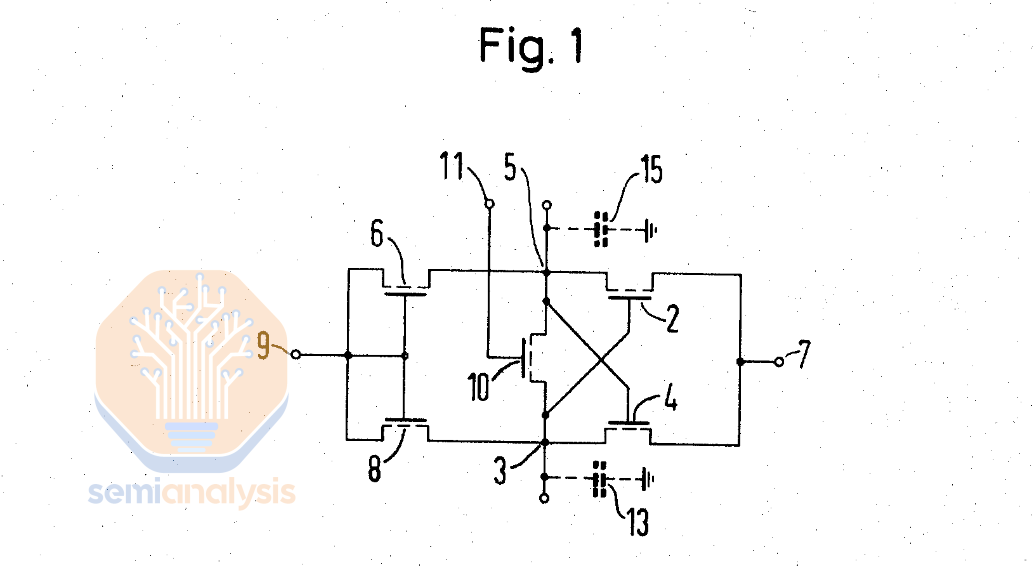
Despite the invention of the 1T1C memory cell structure, early DRAM shipped by Intel in 1973 used 3 transistors per cell with the gate on the middle transistor acting as a storage capacitor. This was a “gain cell” where the middle and final transistor provided gain to amplify the very small charge on the middle gate, enabling the cell to be read easily and without disturbing the stored value. A 1T1C cell is better in theory: fewer devices, simpler to wire together, and smaller. Why was it not immediately adopted? It was not yet practical to read the cell. At the time of invention, the small capacitance of the 1T1C cell made it infeasible to operate. A second key invention was needed: the sense amplifier. The first modern sense amplifier was developed in 1971 by Karl Stein at Siemens, presented at a conference in California, and completely overlooked. The 1T1C architecture was not widely adopted at that point and Siemens had no idea what to do with this invention. Stein was moved to another assignment where he had a successful career unrelated to DRAM.
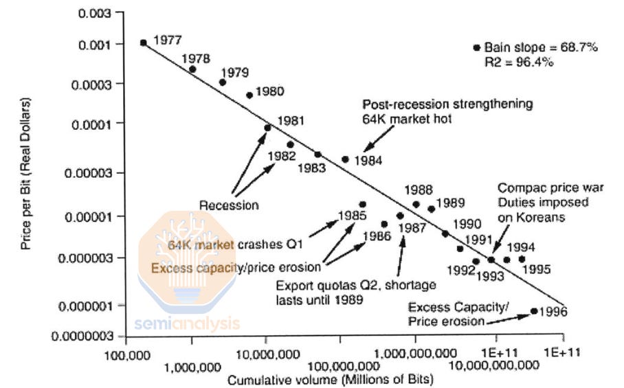
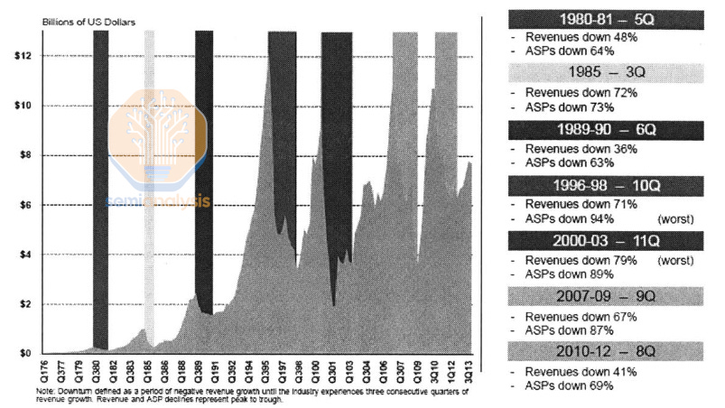
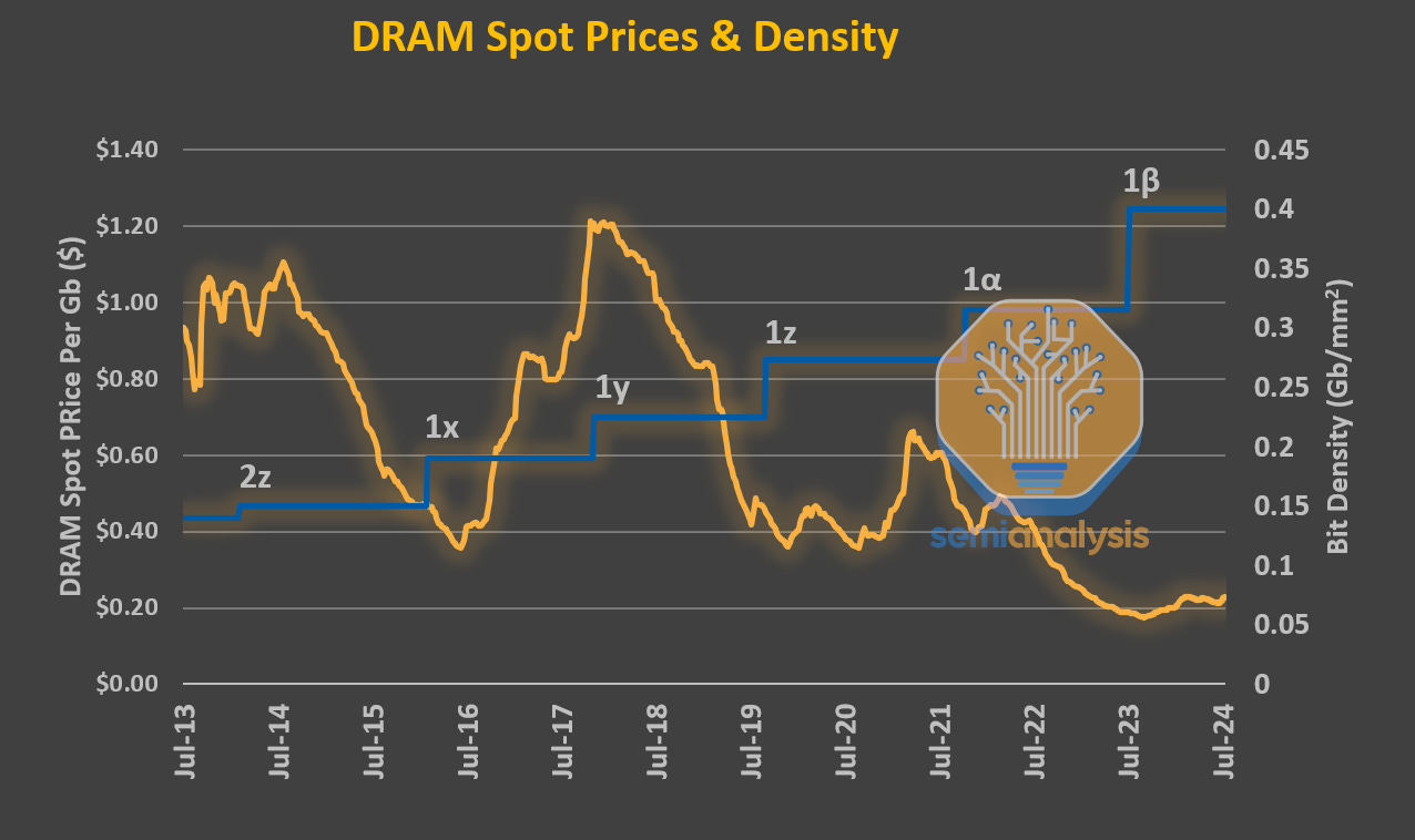
This design was well matched to the spacing of the bit lines and has been able to scale smaller to keep pace with cell size. The sense amp is completely powered down when not in use which allows there to be millions of them on a chip without draining power. They have been a small miracle. It took more than 5 years for the sense amplifier’s time to come. Robert Proebsting at Mostek independently (re)discovered the concept and by 1977 their 16kb DRAM with 1T1C + SA architecture became the market leader. This winning formula stuck – DRAM architecture is fundamentally the same nearly 5 decades later. DRAM Primer: When DRAM Stopped ScalingIn the 20th century, Moore’s Law and Dennard scaling ruled the semiconductor industry. At its zenith, DRAM density increases outpaced logic. DRAM capacity per chip doubled every 18 months, fueling the rise of Japanese fabs (who first exceeded US market share in 1981 and peaked around 80% in 1987) and later Korean companies (whose market share surpassed Japan’s in 1998). The rapid generational replacement of fabs on a relatively simple process created opportunities for new entrants with the funds to build the next generation fab. This pace was not feasible for long, and by the end of the 20th century into the 21st, logic had outpaced memory scaling significantly. Recent logic scaling has slowed to a pace of 30-40% density improvements every 2 years. But this is still good in comparison to DRAM which is roughly an order of magnitude slower than its peak, now needing 10 years for a 2x density increase. This scaling slowdown had knock-on effects in DRAM pricing dynamics. While memory has traditionally been a cyclical industry, slow density scaling has meant much less cost reduction to cushion price increases when supply is limited. The only way to increase DRAM supply is to build new fabs. Wild price swings and high CAPEX mean only the largest companies survive: more than 20 manufacturers produced DRAM in the mid 1990s, with 80% market share spread amongst the top 10. Now the top 3 suppliers own more than 95% of the market. Because DRAM is commoditized, suppliers are inherently much more susceptible to price fluctuations (in contrast to logic or analog) and must compete primarily on the raw prices of their goods when the market is low. Logic has only maintained Moore’s Law with increasing costs, DRAM does not have that luxury. The cost of DRAM is simple to measure, $/Gb. Relative to earlier periods, the last 10 years have seen a slow price decrease – only 1 order of magnitude in a decade when it used to take half that time. The characteristic peak and trough behavior of DRAM is evident as well. Since entering the 10-nm nodes, DRAM bit density has stagnated. Even the addition of EUV in Samsung’s 1z and SK Hynix’s 1a nodes did not significantly increase density. Two notable challenges are in the capacitors and sense amplifiers. Capacitors are difficult in many aspects. First, patterning is demanding as the holes must be tightly packed with very good critical dimension (CD) and overlay control, to contact the access transistors below and avoid bridging or other defects. Capacitors have a very high aspect ratio and etching a straight and narrow hole profile is exceptionally difficult, further compounded by the need for a thicker hardmask to enable a deeper etch as a thicker mask necessitates thicker photoresist which is harder to pattern. Next, multiple defect-free layers of a few nm thickness must be deposited on the walls throughout the hole profile to form the capacitor. Nearly every step strains the limits of modern processing technology. Sense amplifiers are a similar story to logic interconnects. Once an afterthought, they are now of equal or even greater difficulty than the “main” features (logic transistors and memory cells). They are squeezed from multiple sides. Area scaling must be done to match bitline shrink, with the sense amps becoming less sensitive and more prone to variation and leakage as they are made smaller. At the same time, smaller capacitors store less charge, so the sensing requirement to read them becomes more difficult. There are other challenges as well, with the upshot being that scaling DRAM in an economical way is increasingly difficult using traditional approaches. The door is open for new ideas – let’s explore some of them… Short-Term Scaling: 4F2 and Vertical Channel TransistorIn the short-term, DRAM scaling will continue along its traditional roadmap. Larger, fundamental changes to architecture will take years to develop and implement. In the meantime, the industry must respond to the need for better performance, even if only with marginal improvements. The short-term roadmap has 2 innovations: the 4F2 cell layout and vertical channel transistors (VCT).
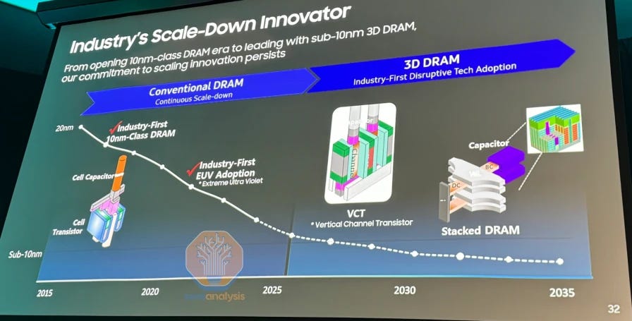
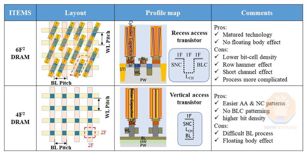
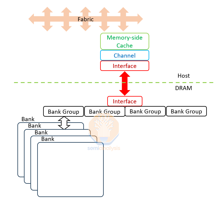
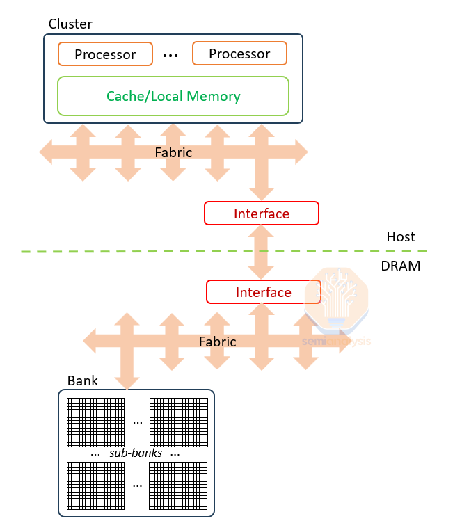
Note that some companies, including Samsung in their roadmap, put VCT under the “3D” banner. While technically true, this is a bit misleading as VCT is distinct from what is commonly called “3D DRAM.” 4F2 describes the memory cell area in terms of the minimum feature size F, similar to the track metric for standard logic cell height e.g. a “6T cell.” The minimum feature size is generally the line or space width, in DRAM this will be the wordline or bitline width. It’s a simple way to denote the density of a cell layout and makes comparison easy – a 4F2 cell is only 2/3rds the size of a 6F2 cell, offering a theoretical 30% density increase without scaling the minimum feature size. Note that pure cell layout is not the only limit to density scaling, so the real benefits are likely to be less than the ideal 30% case. 4F2 is the theoretical limit for a single bit cell. Recall that feature size is the line or space width (i.e. the half pitch), so a line + space pattern will have a pitch of 2F, not F, and thus the minimum possible cell size is 4F2 not just F2. So once this architecture is achieved, the only avenue for horizontal scaling is to scale F itself – something that is rapidly becoming impractical, if not outright impossible. DRAM has used a 6F2 layout since 2007, with 8F2 before that (interesting aside: modern NAND already uses a 4F2 cell but with a significantly larger feature size F. SRAM is on the order of 120 F2, 20x less dense!) One notable exception is CXMT, a Chinese vendor which used VCTs and a 4F2 layout in their sanctions busting 18-nm DRAM, demonstrated in late 2023. Because Samsung, SK Hynix, and Micron were able to scale cells, they were not forced to adopt these architectures in the same way that CXMT was. The implication of CXMT’s early adoption is also important – it is likely they are having difficulty scaling F as they opted for the more drastic change in cell and transistor architectures. The key enabler for 4F2 cells is the vertical channel transistor. It’s necessary simply because the transistor must scale down to fit in the cell and both contacts – to bitline and to capacitor – must also fit in that footprint, so, one vertical line. At these scales it becomes necessary to construct the transistor vertically instead of horizontally, reducing its footprint down to roughly 1F, roughly matching the capacitor above it, while maintaining enough channel length for the transistor to operate effectively. Current DRAM uses horizontal channels and source/drains with horizontal separation. These are a mature and well understood architecture. VCTs stack a source (connected to the BL below it), channel (surrounded by gate & the wordline controlling the gate), and drain (connected to the capacitor above) sequentially. There are tradeoffs in fabrication where some steps get easier and others harder, but overall VCTs are more difficult to manufacture. Samsung’s process is notable for the use of wafer bonding. In a process similar to backside power delivery for logic, the cell access transistors are fabricated with bitlines formed on top before flipping the wafer over and bonding to a support wafer, so the bitline is now buried. Interestingly, the bonded base does not seem to need accurate alignment with the VCTs though the disclosure does not explain whether the periphery CMOS will be on the flipped chip, or in the newly bonded base. The topside is thinned to expose the other end of the transistors so the storage capacitors can be built atop them. EVG and TEL stand to gain from this new incremental need for wafer bonding tools. DRAM Primer: Current VariantsDRAM comes in many varieties, each optimized for different goals. The relevant latest-gen flavors are DDR5, LPDDR5X, GDDR6X, and HBM3/E. Differences between them lie almost entirely in the peripheral circuits. The memory cells themselves are similar across varieties and the fabrication methods are broadly similar for all types. Let’s briefly introduce the various DRAM flavors and the role of each. DDR5 (Double Data Rate gen. 5) delivers the highest memory capacity as it is packaged in dual in-line memory modules (DIMMs). LPDDR5X (Low Power DDR5 with X meaning enhanced) provides low-power operation but requires shorter distances and low capacitance connections to the CPU which limit capacity, so it is used in mobile phones and laptops where low power is desirable and the layout constraints tolerable. More recently we have seen higher capacity packaging for LPDDR used in some AI accelerators, Apple’s professional workstations, and AI feeder CPUs such as Grace. These new uses are driven by the search for power efficient data transfers and high bandwidth. In accelerators, LPDDR has emerged as the best option for a “2nd tier” of memory that provides cheaper capacity at a lower (slower) level than expensive HBM. It falls short in building highest capacities and in reliability features, but beats DDR5 DIMMs as it consumes an order of magnitude less energy per bit of throughput. LPDDR5X packaging goes up to 480GB available on the Nvidia Grace processor, which is about 10x the capacity limit for GDDR configurations (which are limited by rules of circuit board layout and chip packaging required to meet signal in consumer gaming systems), and in the same range as medium DDR server configurations. Larger capacity DDR5 is possible using R-DIMMS of size above 128GB, albeit costly due to packaging complexity and the additional Registers (a kind of buffer chip) on the DIMMs. LPDDR5X has a large advantage in power consumption vs. DDR and in cost vs. HBM, but the energy per bit cannot challenge HBM and it requires many lanes (connections to the CPU) which crowd board layouts at larger capacities. It also has a weak story on error correction (ECC) which becomes more important at larger capacities as there is greater chance of an error. To compensate, some capacity must be diverted to support extra ECC. For example, the Grace CPU has 512GB of LPDDR5x per compute tray but seems to reserve 32GB for reliability features, leaving 480GB available for use. The upcoming LPDDR6 standard shows little improvement, retaining high lane counts per chip and relatively mild speed increases along with limited support for error correction. LPDDR6 will not deliver an HBM competitor. GDDR6X (G for Graphics) is focused on graphics applications, offering high bandwidth at low cost but with higher latency and higher power consumption. Although useful in gaming GPUs, it was engineered with board-level capacity limits and power levels that limit the size of AI applications which can use it. Then there is HBM3E (High Bandwidth Memory gen. 3, with an enhanced “E” version). It prioritizes bandwidth and power efficiency but is very expensive. The 2 defining characteristics of HBM are the much wider bus width and the vertically stacked memory die. Individual HBM die have 256 bits each of I/O, 16x more than LPDDR which has a bus width of only 16 bits per chip. Dies are vertically stacked, typically 8 or more, with I/O grouped for every 4 dies; in total the package can deliver 1024 bits of bandwidth. In HBM4 this will double to 2048 bits. To make the most of HBM it is best co-packaged next to the compute engine to reduce latency and energy per bit. To expand capacity while maintaining a short connection to compute, more dies must be added to the stack. The high cost of HBM is mainly driven by this need for die stacking. In a typical HBM stack, 8 or 12 DRAM dies (with 16 and beyond on the roadmap) are stacked atop each other, with power and signal routed by Through Silicon Vias (TSVs) in each die. TSVs are wires passing directly through the chip, that allow connection between chips. TSVs are much denser, more performant, and more costly than the older wire-bonding methods used to connect stacked chips. More than 1,200 signal wires must be routed via TSVs in an HBM stack. Significant area must be dedicated to them, making each HBM DRAM die double the size of a standard DDR die for the same capacity. This also means higher binning requirements for electrical and thermal performance for the DRAM die. This complexity detracts from yield. For example, Samsung’s DRAM design mishaps and their use of a trailing 1α node are contributing to their shockingly poor HBM yields. Packaging is the other major challenge. Properly aligning 8+ die with thousands of connections each is difficult and therefore expensive due to relatively low yields. At the moment this is one of the key differentiators between HBM suppliers, as SK Hynix can successfully produce HBM3E with their MR-MUF packaging while Samsung struggles to yield their product. Micron has a viable solution, but needs to scale production significantly. Despite the high costs and yield challenges HBM3E is, for now, the most valuable and high-margin product the memory industry has ever had. This is primarily because for large-model AI Accelerators, no other flavor of DRAM is a viable alternative. While margins are likely to erode as Samsung improves yield, and Micron as they scale production, the memory appetite of AI accelerators will continue to grow – to some extent offsetting the benefit of this new supply. In short, high bandwidth and very high bandwidth density along with best energy per bit and true ECC capability makes HBM3E the clear winner, for now, for AI Accelerators. This is why products like Nvidia’s H100 and AMD’s MI300X use it. GDDR6/X comes in a distant second by the same metrics albeit with tiny capacity. LPDDR5 and DDR5 are even worse, neither is suited to accelerator needs. The current HBM solution is expensive and will be increasingly difficult to scale. How did we end up in this situation? HBM RoadmapHBM is a packaging solution built around legacy DRAM ideas, but packaged with density and adjacency to try to solve the bandwidth and power problems for AI and other forms of high-performance computing. All leading AI GPUs now use HBM as their memory. Plans for 2025 have 12-Hi HBM3e with 32 Gb chips for a total of 48 GB per stack, with data rate to 8 Gbps per wire. In GPU servers the first versions of unified memory with a supporting CPU have launched with AMD’s MI300A and Nvidia’s Grace Hopper. The Grace CPU has high capacity LPDDR5X, while the GPU has high bandwidth HBM3. However, the CPU and GPU are on separate packages, connected over NVLink-C2C at 900 GB/s. This model is simpler to integrate but more difficult on the software side. The latency of memory connected to the other chip is much higher and could affect a significant number of workloads. As such, the memory is not quite uniform and comes with its own challenges. 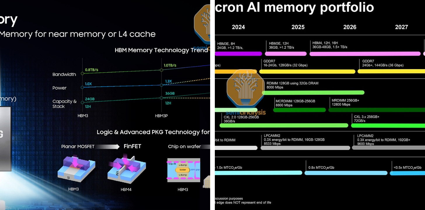 Source: Samsung, Micron HBM4 is a few years away, with Samsung and Micron claiming it will be up to 16-Hi with 1.5 TB/s per stack. This is more than twice the bandwidth of what we have today at only 1.3-1.5x the power, but this scaling is not enough, as the power consumption of memory continues to increase overall. HBM4 will also change to 2048-bit width per stack, reducing data rates by a small amount to 7.5 Gbps, helping with power consumption and signal integrity. It is likely that the data rates will increase to the levels of HBM3E with HBM4E or something similar. The other significant change is in the HBM base die. The base die will be fabricated on FinFET processes as opposed to the planar CMOS technology used now. For Micron and SK Hynix who do not have this logic capability, the base die will be fabricated by a foundry with TSMC already making announcements that they will be the partner for SK Hynix. Additionally, there will be customization of the base die for individual customers. We have a separate report on HBM customization coming, but a quick primer here: HBM4 announcements predict that at least 2 different forms of base chip will be in use, allowing the memory interface to be optimized for different speeds and lengths. It is likely that functionality controlling the DRAM state machine will move onto the base chip to more efficiently control the DRAM chips, and the vertical-only connections may allow energy per bit to be reduced. Custom HBM can enable multiple other package architectures outside of the conventional CoWoS-based assemblies we see today. There could be repeater PHY to daisy chain multiple rows of HBM -though anything beyond 2 ranks would see diminishing returns. With HBM4 and successors, the move to hybrid bonding has been suggested. This will allow for thinner HBM stacks as the bump gap is removed, and improved heat dissipation. Moreover, it will allow for stack heights of 16-20+ layers. It may also reduce power consumption by a small amount as the physical distance that signals travel will be reduced. The challenges are substantial though – yielding a bonded stack of 16+ die, none perfectly flat, is not easy – nobody is close to a high volume manufacturing-ready solution here. All initial HBM4 will not use hybrid bonding, and we expect that to remain true for much longer than most would hope. The connection between the CPU, GPU or accelerator, and memory is in the base chip. Improving this connection is one possible avenue for overcoming memory limitations. Eliyan, a startup funded by Micron and Intel amongst others, is spearheading this approach with their UMI custom interface. 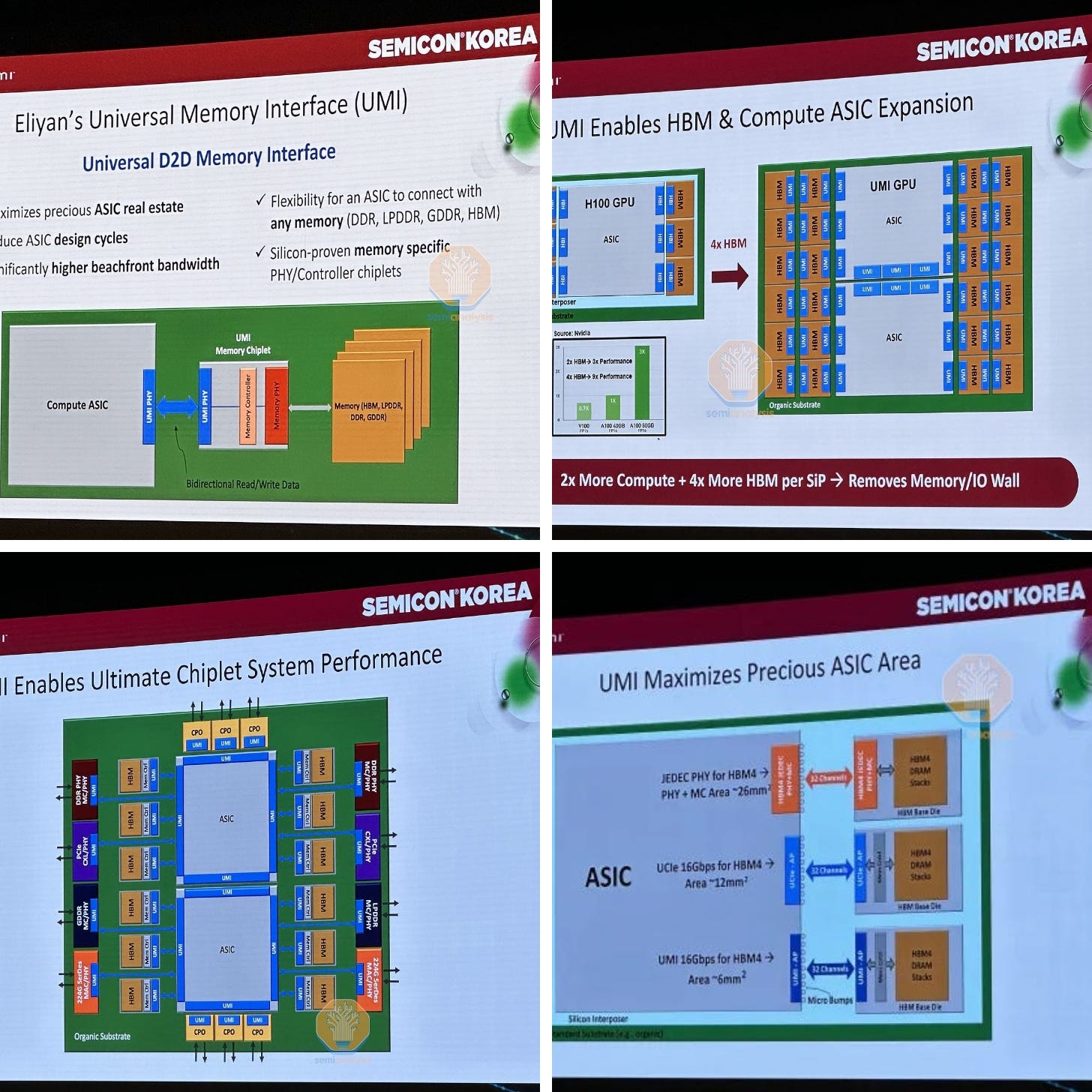 Source: Eliyan This UMI interface is used with an ASIC die, which acts as the base chip for an HBM stack or a module controller for other memory types. This chiplet contains both the memory controller and physical interconnect (PHY) to the memory chips. The UMI connects externally to the host GPU, attaching to the fabric of the host. Manufactured with a full CMOS process they can be fast and efficient, using an advanced “Nulink” protocol to connect to the host and eliminate the memory controller footprint from the host silicon. Eliyan’s packaging technologies work even with standard substrates and have much further reach than regular advanced packaging. This may allow for HBM that is not adjacent to the ASIC die, but much further away, meaning higher capacities can be accommodated. Their approach also uses less area and shoreline on the host which means that the channel width can be increased. Standardized UMI memory chiplets could allow for HBM, DDR, CXL memory and more to be used without being fixed to a specific type, increasing flexibility significantly. While it’s possible this approach may offer short-term improvements, it does not address the underlying cost issues with HBM. Emerging MemoryFor as long as DRAM and NAND have been incumbent, there has been research into better alternatives. The umbrella term for these is “emerging memories.” It’s a bit of a misnomer as, so far, none of them have managed to “emerge” into a high volume product. Given the new challenges and incentives surrounding AI though, they’re worth at least a short discussion. The most promising memory for discrete applications is FeRAM. Instead of using a dielectric (insulating material) in the storage capacitor, they use a ferroelectric (a material that polarizes in an electric field). These have the desirable characteristic of being non-volatile i.e. they can store data when turned off and do not waste power or time on refreshes. Micron showed promising results at IEDM 2023 with density comparable to their D1β DRAM along with good endurance and retention performance. In other words a good candidate for AI/ML use if it weren’t for one issue: cost. It is complex to manufacture and makes more use of exotic materials than conventional DRAM, to the point that it simply is not competitive at present. MRAM is another promising research area. Instead of using electrical charges, data is stored by magnetic means. Most designs use magnetic tunnel junctions (MTJ) as the bit storage cell. At IEDM 2022, SK Hynix and Kioxia showed off a 1-selector MTJ cell with a 45nm pitch and 20nm critical dimension. Together, they achieved the highest MRAM density to date of 0.49 Gb/mm2, greater than Micron’s D1β DRAM which has a density of 0.435 Gb/mm2. The cell even features a 4F2 design. Their aim is to productize in discrete packages as an alternative to DRAM. At present none of the alternative memories are well placed to challenge DRAM. Some have larger or slower cells. Some have more expensive processes. Most have limited endurance. Some have low yield. In practice, the products shipping for magnetic or phase change memories are sized in MB not GB. This could change, there is a lot of money at stake and a winning combination may exist in stealth, but there is a lot of work on both devices and on scale of production to be done. Compute In MemoryDRAM has been hamstrung from the beginning by its architecture. It is a simple state machine without any control logic, which helps keep the cost low, but means it depends upon the host (CPU) to control it. This paradigm is firmly entrenched: modern DRAM fabrication processes are so heavily optimized and specialized that they cannot realistically produce control logic. Industry group JEDEC (Joint Electron Devices Engineering Council) also enforces minimal intrusions from logic when developing new standards. The DRAM chip is totally dependent on the host: all commands are funneled through one shared interface for multiple banks in the memory, on behalf of multiple threads in the host. Each command requires 4 or more steps to be issued with precise timing to keep the DRAM functioning correctly. The DRAM chips don't even have the logic to avoid conflicts. This is exacerbated by using an ancient half-duplex interface: a DRAM chip can read or write data but not both concurrently. The host has an exact model of the DRAM and must predict if the interface should be set to read or write for every clock cycle. Commands and data are sent on separate wires, which reduces timing complexity but increases the wire counts and “beach front” crowding on the GPU or CPU. Overall, the memory interface has dropped an order of magnitude below the bit rates, beach density, and efficiency of alternative PHYs used by logic chips. The upshot of these disadvantages is that DDR5 DIMMs, the most common on servers, expend more than 99% of read or write energy in the host controller and interface. Other variants are slightly better – HBM energy use is roughly 95% interface, 5% memory cell read/write – but still nowhere near the full potential of DRAM. Functionality is simply in the wrong place. Naturally, the solution is to move it to the correct one: the control logic should be on-chip with the memory. This is Compute in Memory (CIM). Compute in Memory: Unleash the BanksDRAM banks have incredible performance potential that goes almost completely to waste because of interfaces. Banks are the basic unit of DRAM construction. They comprise 8 sub-banks each with 64Mb (8k rows by 8k bits) of memory. The bank activates and refreshes 1 row of 8k bits at once but transfers just 256 of them in or out in any I/O operation. This limitation is due to external connections from sense amplifiers: while the row is supported by 8k sense amplifiers, only 1 in 32 sense amplifiers (256) are connected out of the sub-bank, meaning read or write operation are limited to 256 bits
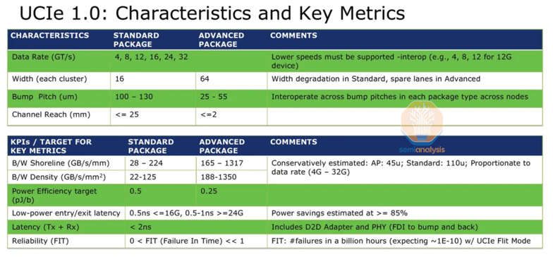
The sense amps are in a canyon surrounded by tall capacitors. In the FIB teardown above from ETH Zurich you can see there is wiring at higher levels which needs tall vias stretching down to make contacts to the sense amps. Even with this limited interface, 1 in 32 accessible at any one time, the peak read/write capacity of a bank is roughly 256Gb/s, with an average closer to 128 Gb/s as at least 50% of time is used in switching to a new active row. With 32 banks per 16Gb chip the full potential of one chip is 4TB/s. Further up the hierarchy, banks are connected in bank groups, which in turn connect to the interface out of the DRAM chip. In HBM, each die has 256 data lines with a peak throughput of 256 GB/s per die. This bottleneck can utilize only 1/16th of the underlying potential of the banks. To add insult to injury, 2pJ of energy are needed to transfer a single bit out of the chip, 20x more than it took to move it in or out of the cell. Most of that happens at the two interfaces on each end of the DQ (Data Question-mark, a data line which is used for both read and write) wires, and in the controller logic on the host. With such a wasteful architecture, it’s inevitable that efforts will be made to access more of the potential performance. Compute in Memory: The Full Potential of DRAMEven simple theoretical examples show there is massive potential on offer here. Implementing the UCIe (Universal Chiplet Interconnect) standard would allow for 11 Tbps throughput per mm of edge – nearly 12x better than HBM3E. Energy per bit would go down by an order of magnitude from 2pJ to 0.25pJ. And UCIe is not even the latest solution… Eliyan’s proprietary Nulink standard, to take just one example, claims even greater improvements. The caveat here is that if the host fabric is extended across the interface, then a subset of the fabric command set must be handled on the DRAM side. Each bank would need to implement the state machine (pre-charge, address select, activate, read/write, close, etc.) locally. This requires (relatively) complex logic fabricated on-chip with the DRAM. Compute in Memory: Path Forward & Possible WinnersAdding logic to a DRAM chip is, of course, no simple task. The good news is that HBM includes a CMOS base chip, and when 3D DRAM arrives there is a virtual certainty that good CMOS logic is bonded atop or underneath the memory stack. In other words, the architecture is amenable to including some compute within memory, and chipmakers will be incentivized to do so. There is low hanging fruit here: consider what could be done if HBM adopted the GDDR7 rate of 32Gbps per data wire. GDDR7 demonstrates that fast enough transistors can be made on the DRAM chips, and the vertical distance through the TSVs to the base stack is under 1mm which should keep energy per bit in the 0.25pJ/bit range. It begs the question: why would JEDEC not lean into an improved standard here? The external interfaces on the base chip could be substantially upgraded to modern designs offering more than a terabyte/sec per mm of edge, at fractional pJ energy per bit. Someone is going to win big in the IP wars. While it’s possible that JEDEC will adopt one choice as standard, more likely it will be done by faster-moving memory / GPU-vendor pairs, as JEDEC usually takes years. We already see real change possible in HBM4 with the acceptance of 3rd party base chips, which is bound to unleash experiments. We will likely see offloaded channel control, pure fabric extension on the interconnect, reduced energy per bit over centimeters of distance, and daisy chaining to other rows of HBM further from the host, or to 2nd tier memory like banks of LPDDR. In this way designs can sidestep the power limits of trying to do compute inside the memory stack and instead use a modernized interface on the base chip to allow neighboring chips the bandwidth and low energy per bit for compute as-if in memory. Below we’ll cover the coming revolution in DRAM: 3D. This will mean a tectonic shift for the memory manufacturers and wafer fab equipment - we’ll discuss basics, how it’s manufactured, and likely winners (and losers). 3D DRAM: Basics...Subscribe to SemiAnalysis to unlock the rest.Become a paying subscriber of SemiAnalysis to get access to this post and other subscriber-only content. A subscription gets you:
|

