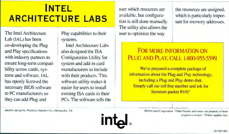
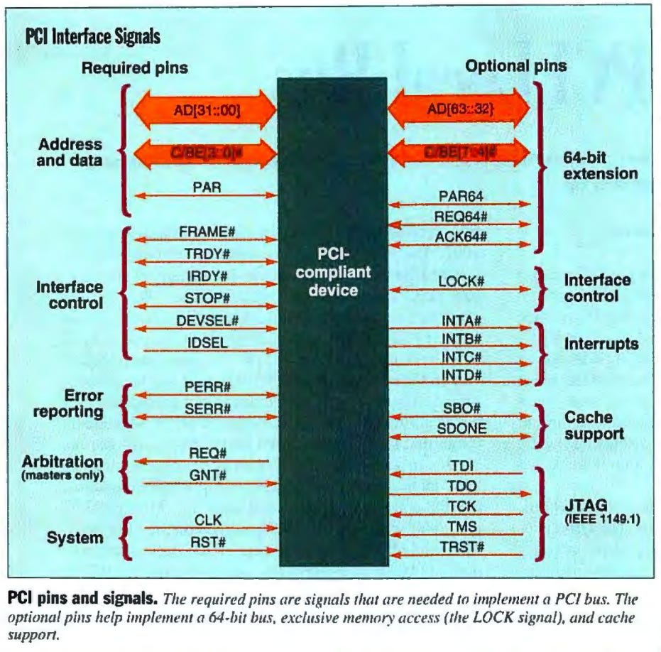
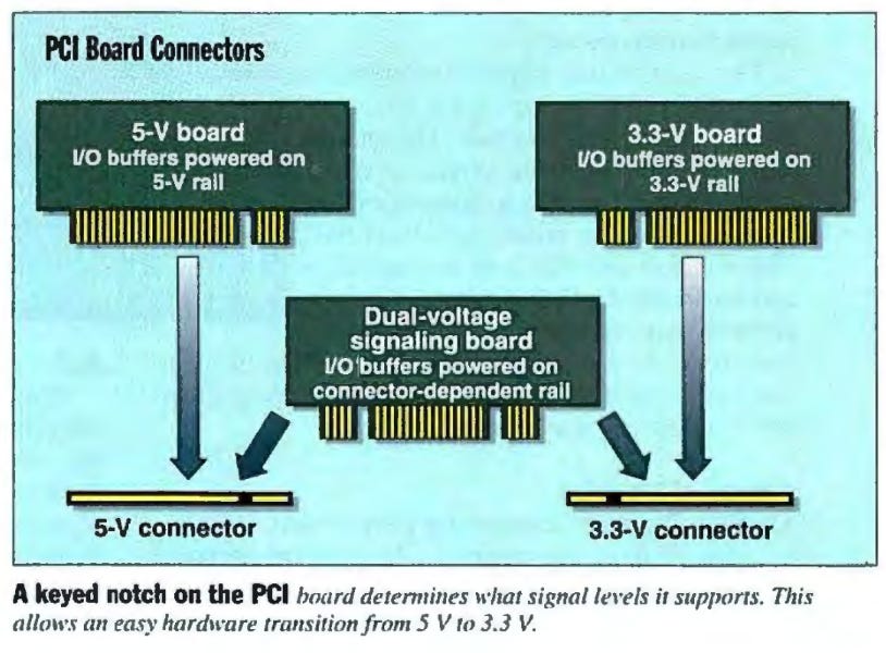
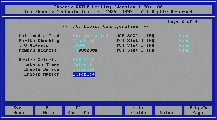
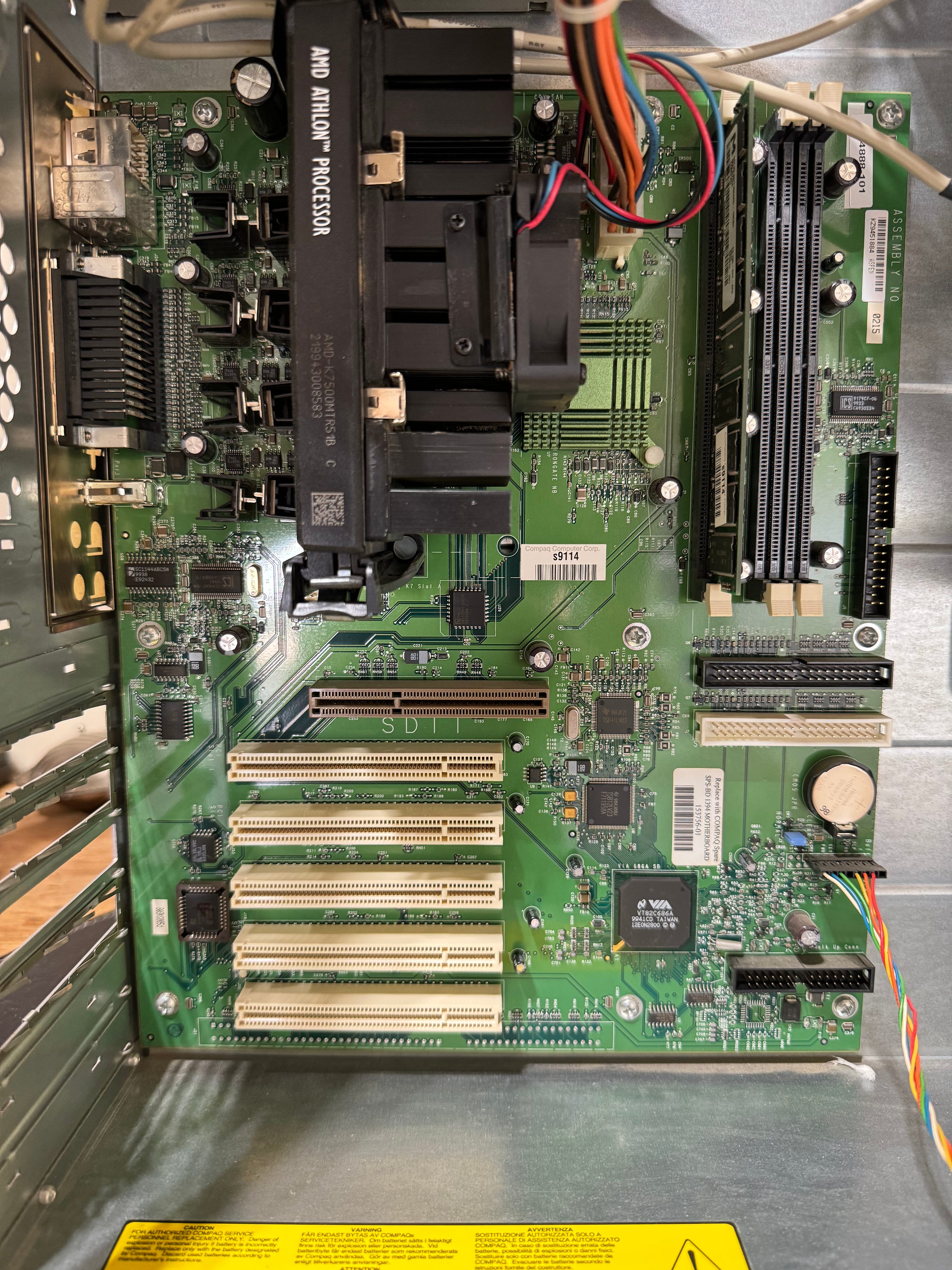
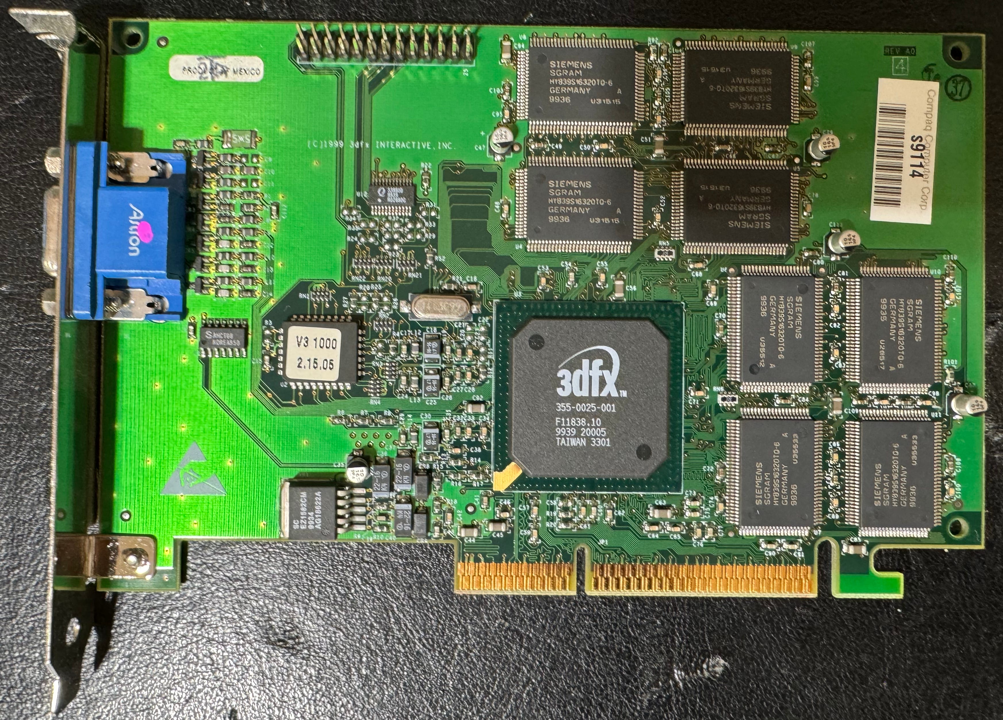
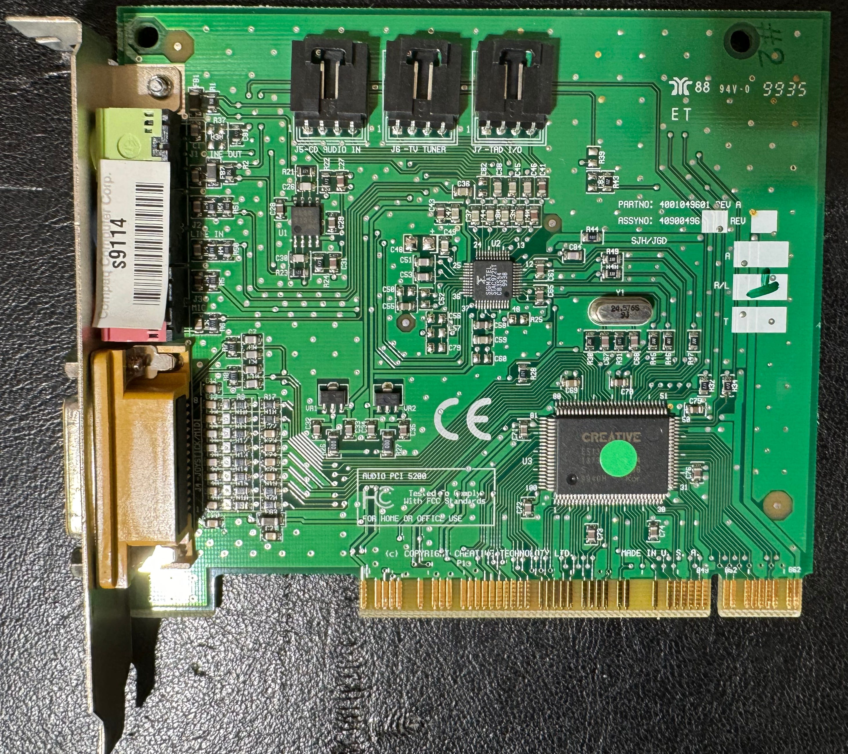
In early PCs, the PC bus ran at whatever the CPU speed was. Originally, this would have meant 4.77MHz. With later revisions of the 8088, this would have meant 6MHz or 8MHz. With the arrival of the NEC V20, this could have meant 16MHz. Cards for the PC bus, however, couldn’t always operate at these frequencies, and therefore later iterations featured separate clocks for the CPU and PC bus. The AT bus operated at 6MHz while later versions operated at 8MHz. Being 16bits wide, the AT bus at 8MHz requiring a minimum of two clock cycles per data transfer would yield a theoretical maximum bandwidth of 8 mbps. In practice, typical throughput would be nearly half of this speed. Still, this didn’t matter at the time the bus standards were created as most peripherals were slow and used little data: serial ports, floppy controllers, keyboard controllers, tape drives, printers. As technology advanced, particularly audio, video, and storage, the limitations of the ISA bus (both the 8bit PC bus and the 16bit AT bus) became more readily apparent, and people began working on replacements. By the late 1980s, there were two different 32bit bus standards. There was IBM’s MCA, and there was EISA led by Compaq. This situation didn’t immediately improve. The VL-Bus emerged for those who needed some serious speed. EISA and VLB were backwards compatible with 16bit ISA, but both had issues and weren’t at all compatible with one another. For EISA, the main problem was a speed of just 8.33MHz. VLB had more serious problems. First, VLB was designed around the 80486 memory bus and wasn’t easily portable to other CPUs. Second, being tied to the memory bus, a system could not have more than two or three VLB devices at once. Finally, VLB had no intermediary between cards. If two devices write to the same memory location, data corruption will result as the system has no method for intervention. It is noteworthy that despite the initial design being for the Intel 80486, a VL-Bus interface was created for the MIPS R4000. Between EISA and VL-Bus, many device manufacturers who needed speed chose VL-Bus, and this was largely a cost concern. VL-Bus made use of the cheap 16bit ISA slot connector paired with an MCA slot connector. Beyond pricing, tt was also a simple hardware design that was cheap to implement. Where it became a pain was in the amount of buffering on-card that was required to alleviate CPU load and in the amount of careful design work needed to ensure that traces on a card were as short as possible. So, while EISA and MCA lost to VL-Bus, the old 16bit ISA standard was still the dominant bus. Putting a coprocessor on an ISA card was cheaper, simpler, and often faster than even VL-Bus. For a hard disk controller, just having a large cache on an ISA card could give an old-fashioned AT bus disk controller an edge over a VLB disk controller. Again in the late 1980s and early 1990s, more CPU architectures were starting to arise. The AIM alliance was working on PowerPC, Sun had SPARC, SGI had MIPS, HP had PA-RISC, Motorola had the 68k and 88k chips, and DEC had Alpha. Within the PC world, there were also more competitors: AMD, Cyrix, IBM. Intel itself had i860, and they were working on P5 and P6. Intel, specifically Intel Architecture Labs, wanted to make a bus that would solve the inadequacies of both EISA and VLB while also being completely processor independent. With this new bus, Intel imagined a card purchaser being able to slot the same model of card into a variety of computers using different CPU architectures, from different manufacturers, and in different environments; a feat enabled by the bus having its own processor-independent controller. Given that the PC BIOS would not be present on these others systems, and that various architectural differences could not be foreseen, Intel also need the bus specification to enforce configuration via software rather than BIOS. They called this Plug and Play or PnP. The end user would no longer be required to set IRQs, memory addresses, or DMA channels. A card would identify itself to the system, and the system would then choose a suitable configuration. Together, the controller, the physical bus design, and the card slots were called Peripheral Component Interconnect or PCI. Plug and Play was not unique to PCI, but it was meant to make PCI far easier on the administrators and users of computers. Intel intended PnP to be used even with newer ISA cards while having some limited utility on cards folks already had. IAL began work on the PCI bus standard in 1990, and they first publicly proposed the PCI standard at an Intel Technical Forum in December of 1991. On the 21st of June in 1992, two weeks before VESA unveiled their technology, Intel released their first specification as an open industry standard, and they further stated that they’d been working closely with IBM, Compaq, NCR, and DEC who, together with Intel, formed the PCI Steering Committee. IAL’s first PCI bus standard was a synchronous bridge between the local bus and the CPU with FIFO buffers. It was 33MHz and could be either thirty two bits or sixty four bits wide, and it could queue reads and writes between the CPU and any attached peripheral card. The maximum bandwidth for 32bit PCI was 132 mbps, and for 64bit it was 264 mbps. The first PCI chipset was the 420TX (codenamed Saturn) released in November of 1992 which was built from the 82423TX and 82424TX as the northbridge (communications hub for RAM, CPU, and link to southbridge) with the 82378IB being the southbridge (the I/O controller linking things like the PCI bus, BIOS, ISA, IDE). The northbridge connected to the CPU’s front-side bus or FSB while the southbridge connected to the northbridge. The 420TX chipset was 32bit and was intended for 5V 486 CPUs. Importantly, this southbridge did not have IRQ steering and therefore didn’t support PnP. As result, early PCI motherboards sporting both PCI and ISA in 1992 or 1993 would require the setting of IRQs as well as jumpers to set a PCI master. The first PCI chipset for Pentiums was the 430LX released in March of 1993 supporting an FSB speed of 66MHz, operating at 5V, and utilizing FPM memory of up to 192MB. The 430LX was built of the 82434LX with two 82433LX chips. In April of 1993, Intel released PCI version 2. By the close of the year, over one hundred fifty companies had endorsed PCI including IBM, Adaptec, S3, Compaq, ATI, and DEC. Of course, it was also in 1993 that Apple announced their intention to make use of PCI in all upcoming Macintosh systems (where it replaced NuBus). There were three important pieces to PCI winning the war for the next bus standard so quickly. First, Intel didn’t charge a license fee for it. Second, Intel almost immediately formed the PCI-SIG to continue development and aid hardware vendors in achieving compliance. Third, Intel thoroughly documented the chipset and made it widely available. By late 1994, it was somewhat clear that PCI was winning. The bus had been adopted for use with DEC’s Alpha chips (DEC actually integrated the PCI controller with the DECchip 210066), and the AIM alliance adopted PCI for the PowerPC. For PC hardware, PCI was not immediately a success. Many 80486 boards continued to ship with ISA, and both PCI and VLB were largely restricted to high-end motherboards. The true adoption of PCI came with the Pentium, and it was with Pentium systems that PnP became common as well. With this adoption speeding up, in 1994, a second industry consortium similar to PCI-SIG was formed specifically to extend PCI within telecom, military, and industrial realms, PCI Industrial Computer Manufacturers Group or PICMG. The relatively slow uptake of 32bit microcomputers, newer and faster bus standards, and even newer operating systems was largely economic, but also a bit cultural. On the 19th of October in 1987, the world experienced a stock market crash. Following the crash, the US economy slowed until it dipped into recession in 1991. The economy began a slow recovery in 1992, but the finance industry wasn’t exactly eager to expand credit. On the cultural side, the explosion of the web and Windows 95 was still in the future. For many people, an AT or an XT was still perfectly suitable for their daily grind of word processing, spreadsheets, some gaming, and perhaps a bit of bulletin board access. With those two factors, it’s little surprise that the 486 released in 1989 was still too expensive for many buyers in the early 1990s. This remained true of the Pentium as well following its launch. PCI therefore didn’t enter most homes until the middle of the 1990s. By this time, EISA and VL-Bus which had been common on server and workstation hardware had been thoroughly beaten. Oddly, within the graphics world, the reign of PCI was also quite brief. The late 1990s was an era of rapid graphics development with the likes of 3dfx, and this led to the Accelerated Graphics Port or AGP. AGP was a superset of PCI that didn’t share the PCI bus and instead had a dedicated path to the northbridge. So, while the Voodoo 1 and Voodoo 2 cards were PCI, the Voodoo 3 is more commonly seen in its AGP version. The first AGP chipset was the Intel i440LX for Slot 1 released on the 26th of August in 1997. Socket 7 chipsets from multiple vendors followed the same year. The late 1990s saw pressures combine to accelerate the rate of adoption of new PC technologies, the Web and 3D gaming. The Web encouraged many people to buy computers for the first time. High speed modems, complex web browsers, and advanced operating systems all combined to necessitate things like the Pentium and PCI. Games like Quake and Tomb Raider likewise pushed buyers toward Pentiums and Voodoo cards. The introduction of Windows 3 and then Windows 95 served to lower the barrier to entry for computer users, and this likewise quickened home microcomputer adoption. These were all advancements that came as the economy was leaving recession and entering another boom phase, and consumers were flush with cash. PCI-SIG became an independent non-profit in 2000. The organization’s first standard was published in 2002 with PCI version 2.3. PCI-X version 2 was released in 2003 as was PCI Express. By late 1998, machines similar to this Compaq Presario weren’t uncommon. This particular machine would have been a higher mid-range configuration with an AMD Athlon clocked at 500MHz, a 3dfx Voodoo 3 1000, and Creative AudioPCI 5200. The machine shipped with either 64MB or 128MB of RAM and was expandable to 384MB. The inclusion of the AudioPCI is the noteworthy component in this Compaq as it’s quite symbolic of the time period in question. This was the last sound card released by Ensoniq before its acquisition by Creative. It supported modern technologies like MS DirectSound3D, but it could also still be used in MS-DOS where it would emulate a SoundBlaster Pro. I have readers from many of the companies whose history I cover, and many of you were present for time periods I cover. A few of you are mentioned by name in my articles. All corrections to the record are welcome; feel free to leave a comment. You're currently a free subscriber to Abort Retry Fail. For the full experience, upgrade your subscription. |
